


Ceramic Tapes & Substrates
Technical ceramics
KERAFOL® is a specialist in the field of technical ceramics. Thanks to our decades of experience, state-of-the-art process technologies, and manufacturing facilities, we are able to provide you with highly technical and high-quality products.
Our experts in the field of technical ceramics develop high-performance and efficient solutions according to your requirements.
Benefit from our experience in the development, manufacturing and distribution of products made of ceramic materials.
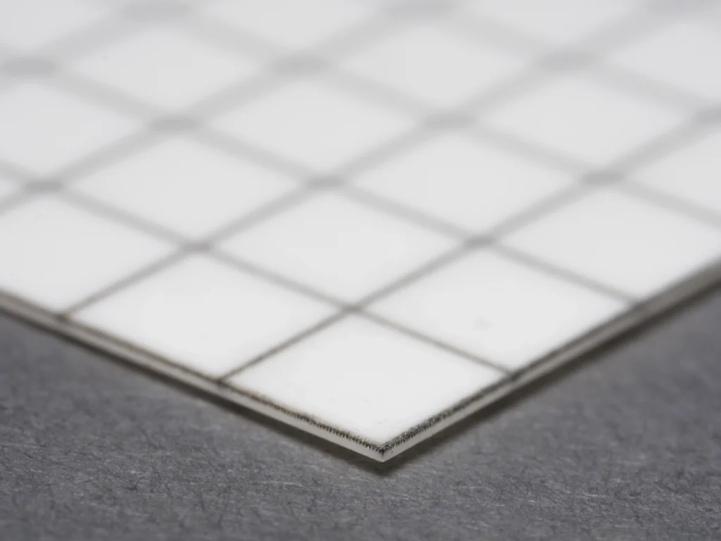
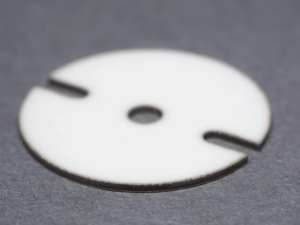
Special ceramic tapes and substrates are ceramic materials for components used in electronics, sensor technology (lambda sensor), as setter plates, in mechanical wear protection technology, in high-temperature fuel cells and in medical technology.
Video: Ceramic Tapes Substrates
Main features
CTS by KERAFOL®
- Excellent high temperature resistance
- Good corrosion resistance
- High mechanical strength
- Low weight
- Low space requirement
- Low heat capacity
- Great hardness
- Very good mechanical abrasion resistance
- Good flexibility of thin ceramic substrates
- Depending on the material, good to very good thermal conductivity
- Very good electrical insulation properties
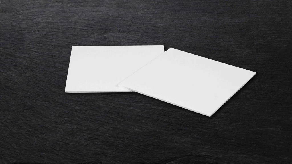
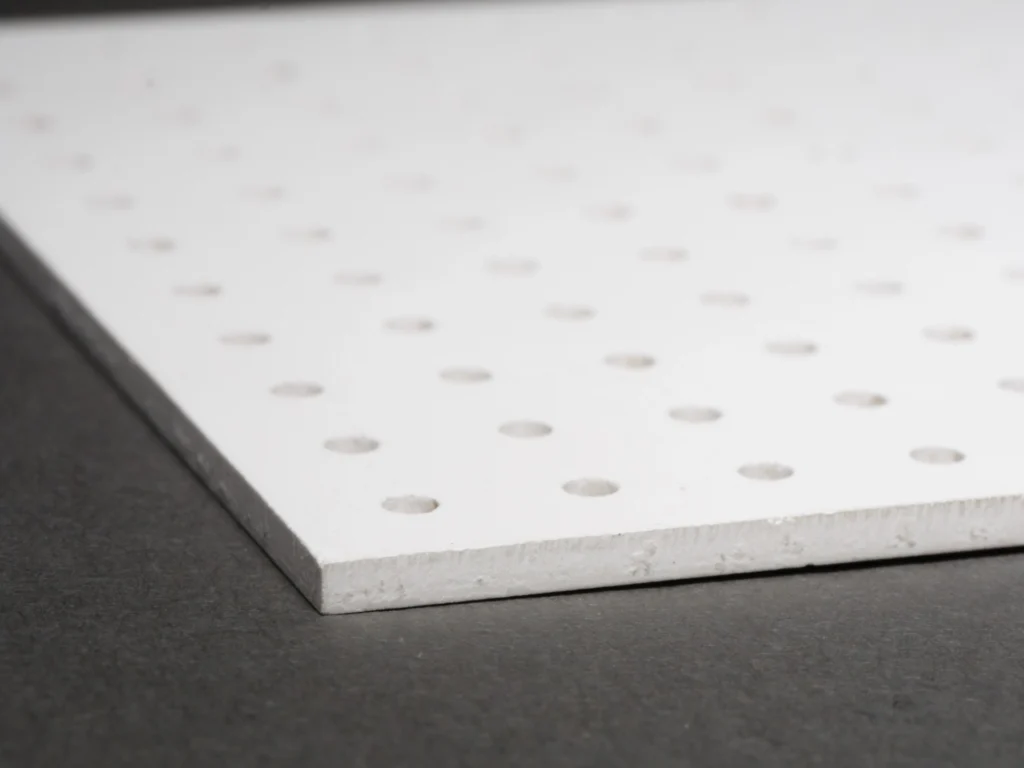
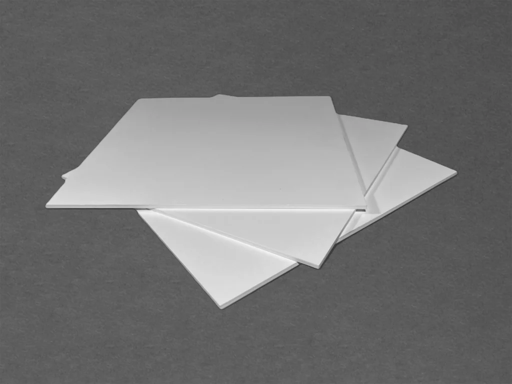
Setter / kiln furniture
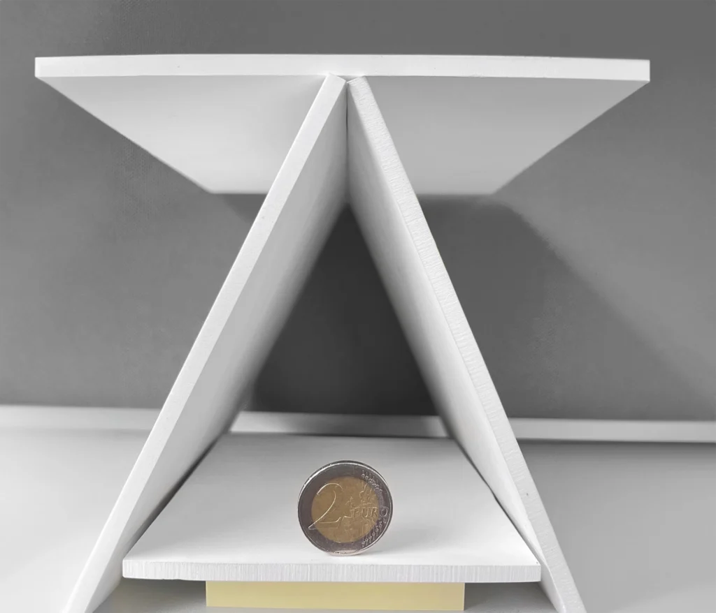
KERAFOL® manufactures sintering aids for high-quality customer products with stringent requirements regarding geometry and material quality.KERAFOL® ceramic plates are manufactured exclusively using the film casting process. As a result, the ceramic plates feature a homogeneous particle distribution within the sintering support matrix. For this reason, the pore distribution and pore size are also homogeneous across the entire ceramic plate.
KERAFOL® sintering aids are therefore ideally suited as sintering supports for the heat treatment of components in MIM, CIM, dental ceramics, PZT, or SOFC ceramic manufacturing.
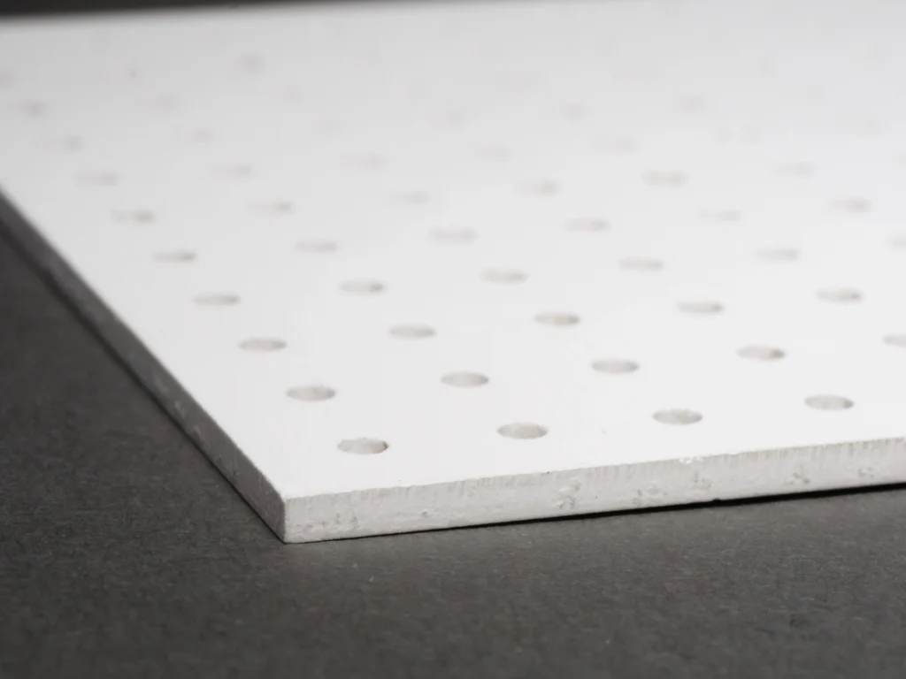
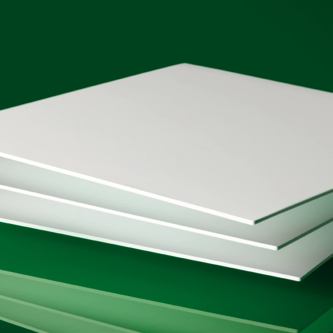
-Thin- and thickfilm-substrates
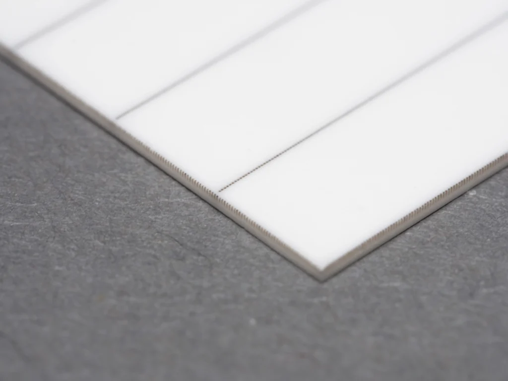
Thinfilm technology
Conductive circuits that are produced using thinfilm technology have layer thicknesses ranging from a few nanometers (monolayer) to several micrometers. Electronic semiconductor components and special platinum temperature sensors (Pt 100, Pt 1000, etc.) are the most important applications in the field of thinfilm technology. The average thickness of the conductive circuits is approx. 1 µm. The conductive circuits for thinfilm substrates are applied at approx. 1200°C using the PVD process or sputtering. The substrates for thinfilm technology are therefore subject to stringent requirements in terms of the surface quality and grain structure of the ceramic.
Thickfilm technology
Thickfilm technology is used to build electronic components such as sensors or embedded hybrid circuits using LTCC or HTCC technology.
The electrical conductors for thickfilm coating technology are applied to the tape or substrate material using a screen printing process.
Wear protection ceramics
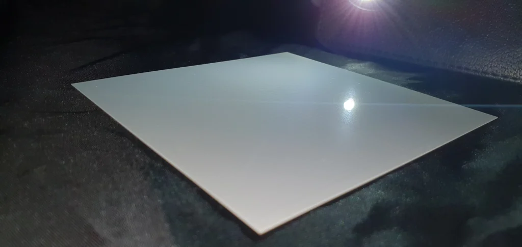
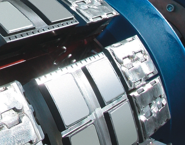
KERAFOL® offers a special and thin ceramic substrate for wear protection applications.
Due to its excellent frictional properties, the material is characterized by high wear resistance and very good sliding properties. It is mainly used for applications where metal and plastic are overloaded and the surface area and weight of the protected section are limited.
Contact person
Do you have any questions, requests or suggestions? How can we help you?
Franz-Martin Fuchs, M.Eng., & Christian Münch, M.S. in Physics
Division Manager, Technical Ceramics
Phone: +49(0) 9645 – 88 430 / +49(0) 9645 – 88 610
Email: keramik@kerafol.com